Reverse-Engineering the Casio SK-1, part 1: Dumping the ROM
When I was younger, I had a Casio SK-1 keyboard that I had a ton of fun with. Of course, I found out about “Circuit Bending,” and in short order, my keyboard was no longer functional.
The Casio SK-1 is famously modifiable, its simple electronics making all manner of sounds when fed unexpected data across its 8-bit data bus, however, given my previous experience years before, rather than circuit-bending the instrument, I decided that I was going to reverse-engineer the data formats used. In theory, this will allow me to program the keyboard myself, rather than feeding it garbage data and using trial-and-error to find something that sounds interesting.
Disclaimer: I have absolutely no clue what I am doing.
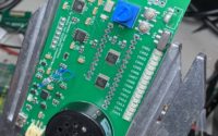
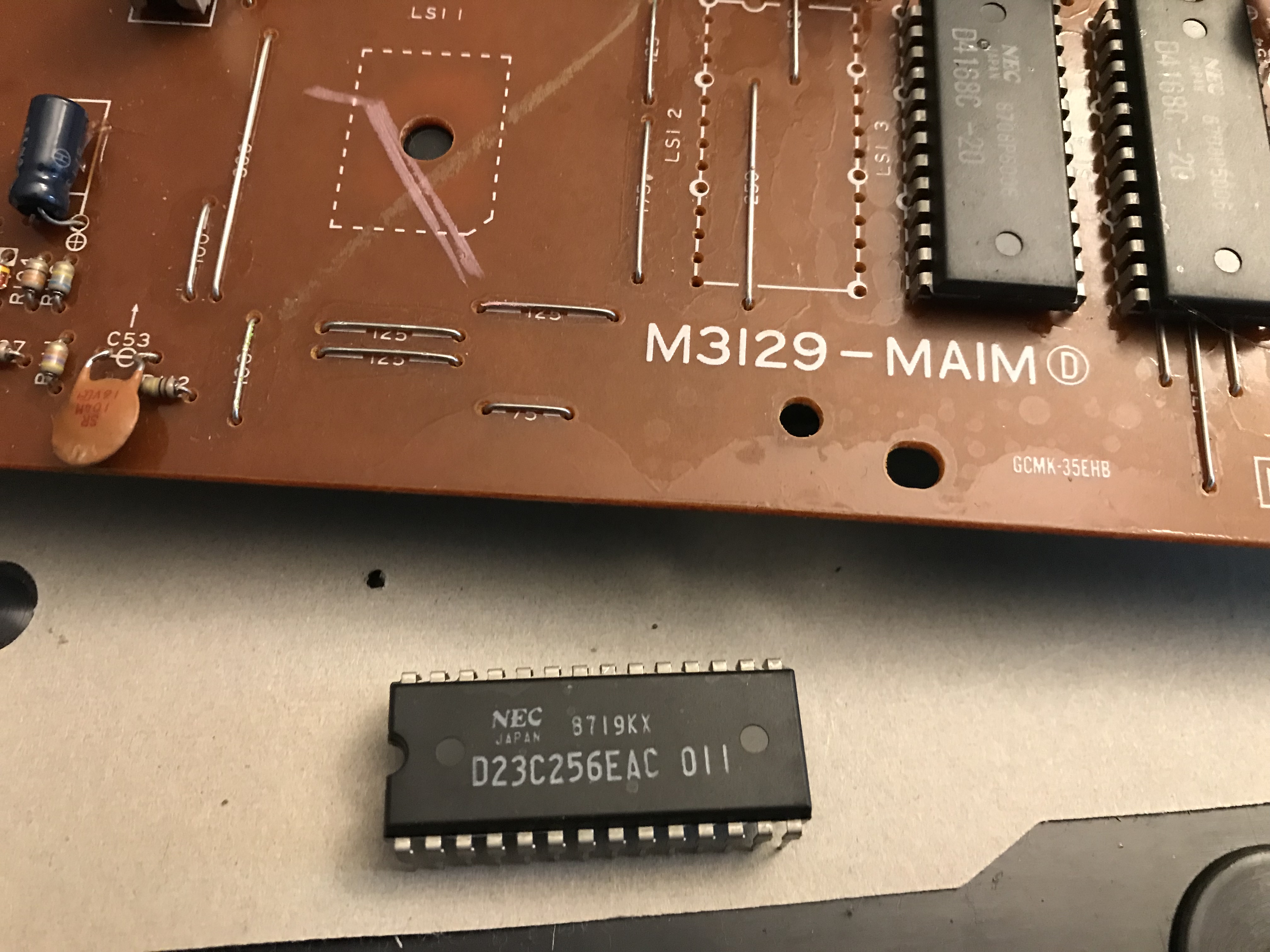
Once inside the unit, three chips became immediately apparent – two 8K RAM chips and one 32K ROM. My assumption here is that sampler recordings and other settings are temporarily stored in RAM, and the ROM contains the patch data we care about.

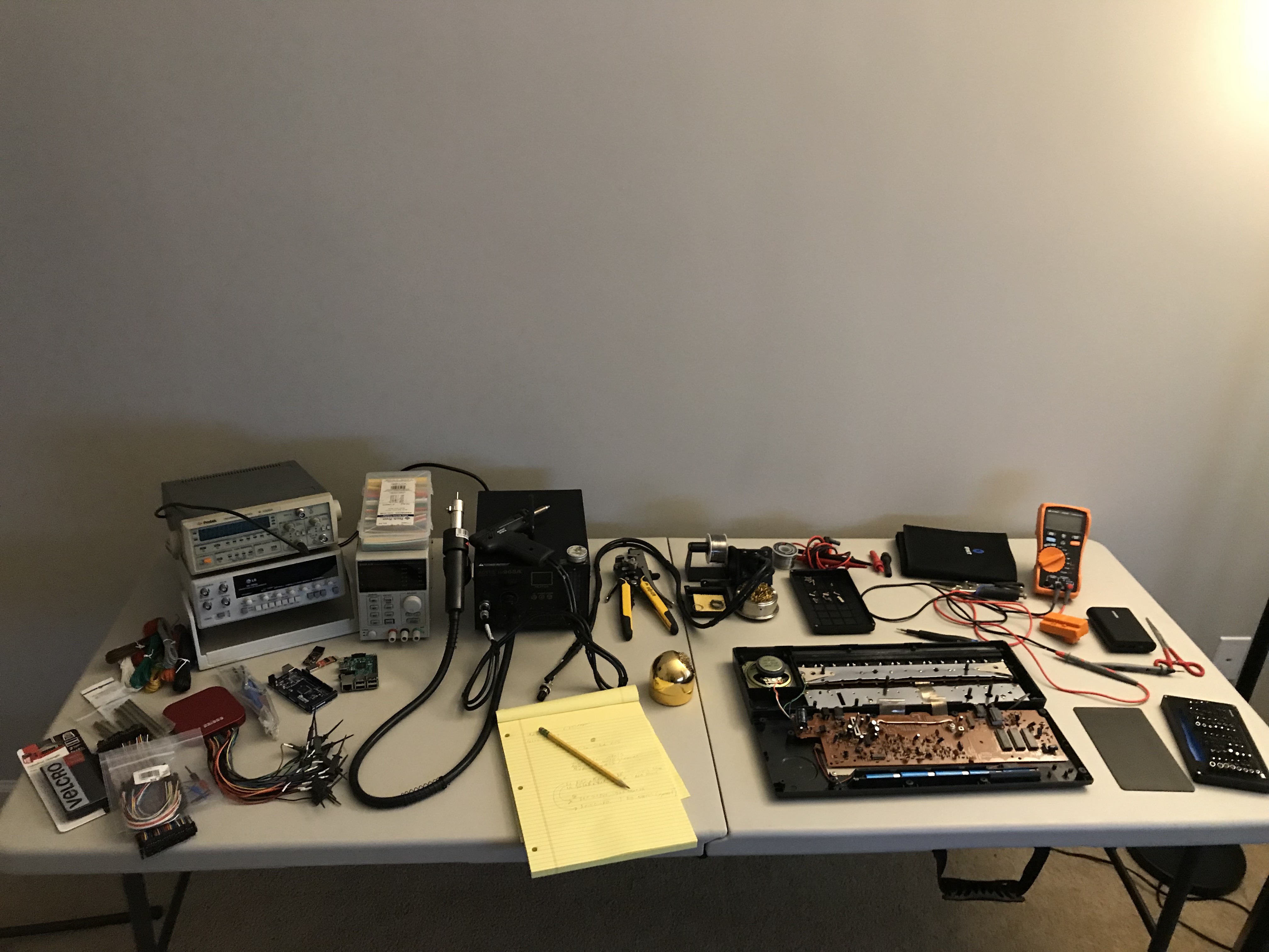
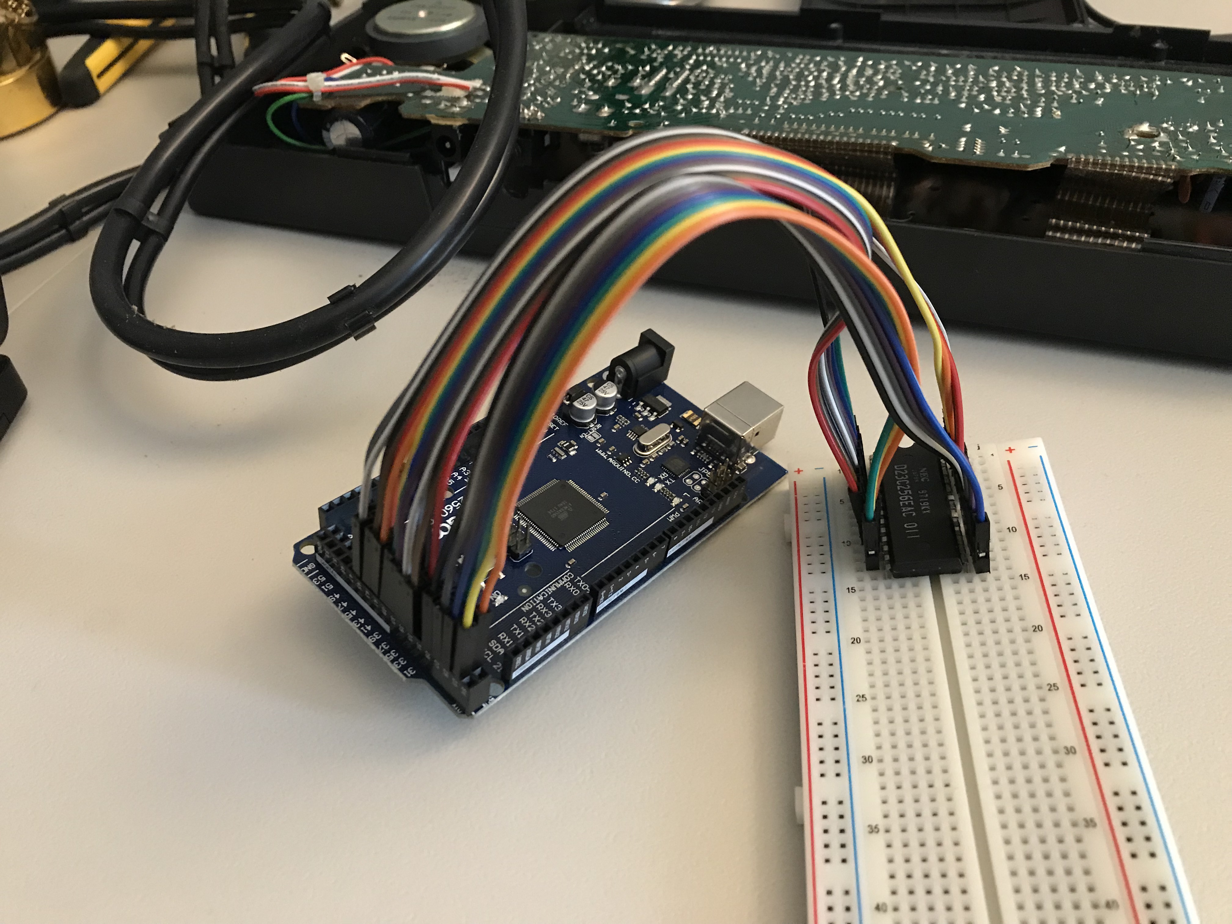
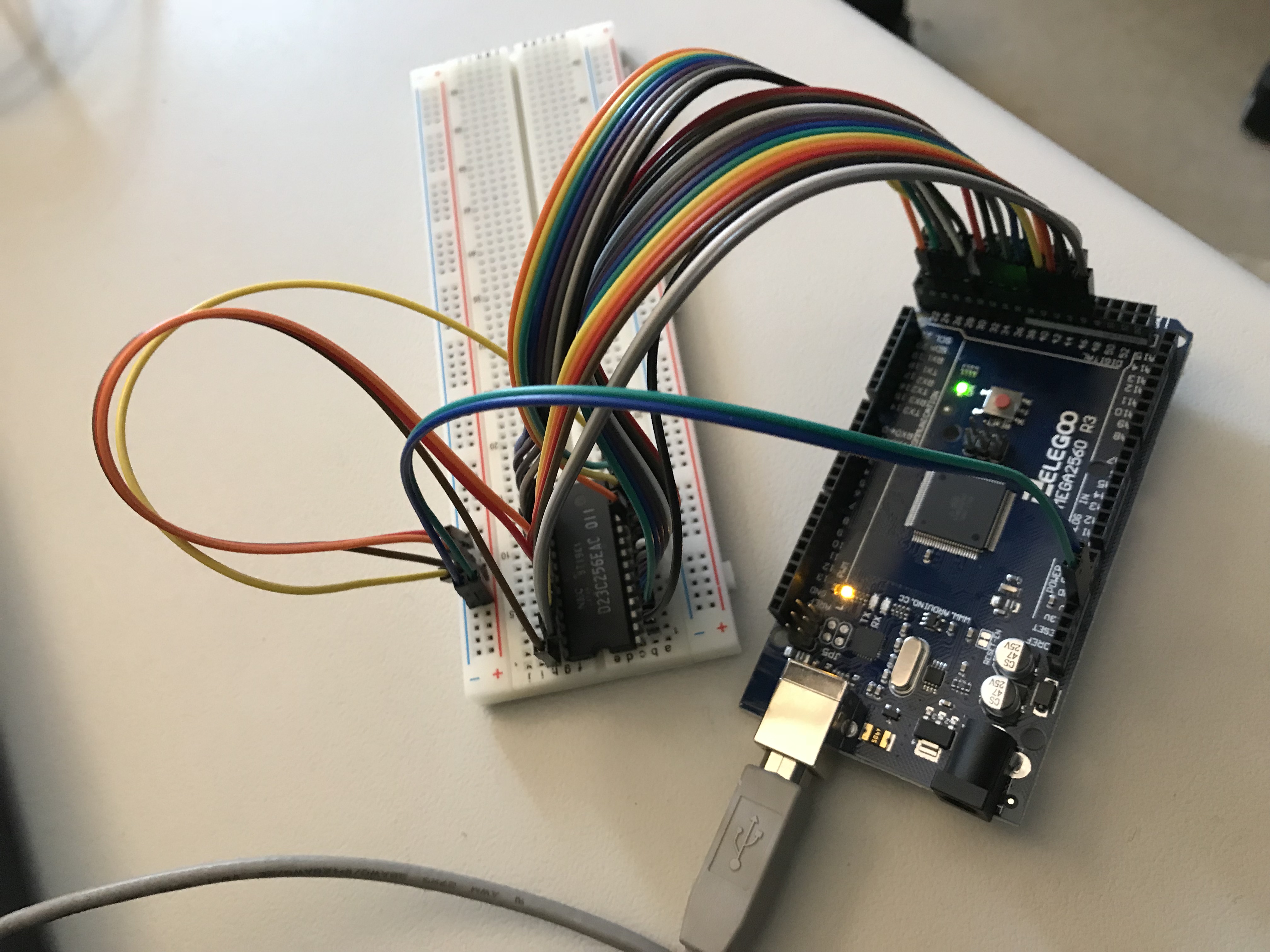
Now that we’ve identified the chip we want to dump, we’ll remove it from the board and hook it up to a microcontroller to read the data.
Now, let’s check the pinout and put it in a breadboard. (I couldn’t find any breadboards in my house and was almost lazy enough to hook leads directly to the pins. I ended up going down the street and spending the $5 and grabbing a breadboard.)

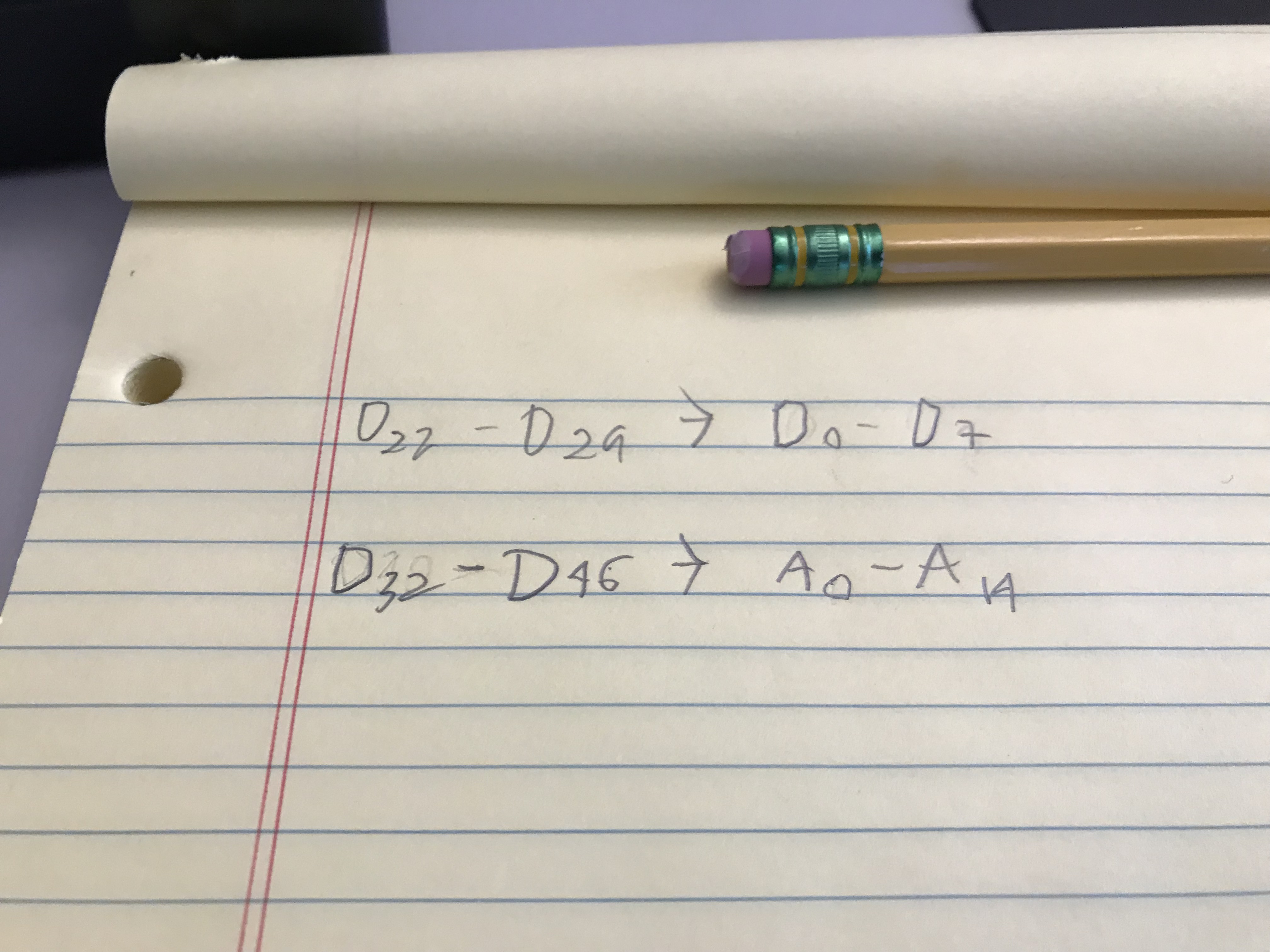
To make things simple, I mapped blocks of digital I/O pins on an Arduino MEGA to the data and address pins on the ROM.
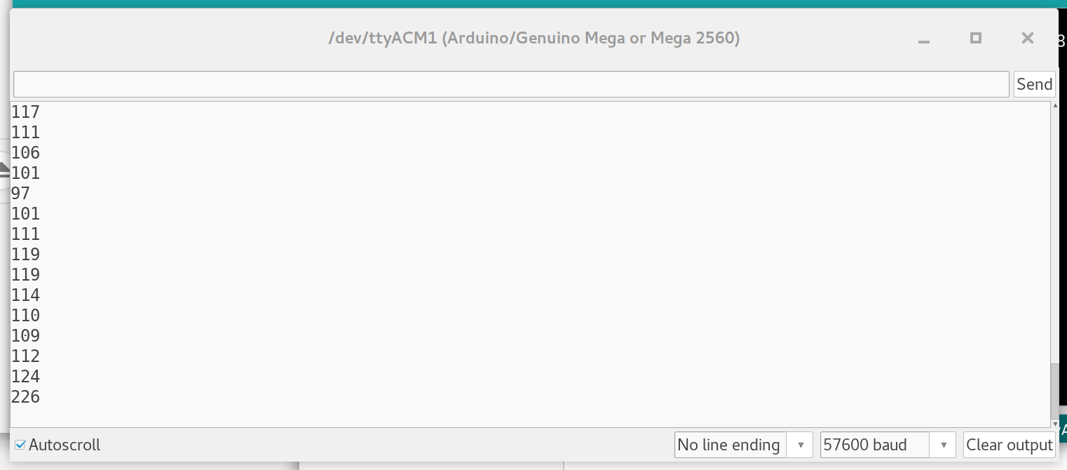
I wrote a little bit of code to use the Arduino to dump the ROM:
(Pretty sure I used the wrong types in a bunch of places but it works)
//D22-D29 => D0-D7
//D32-D46 => A0-A14

void setup() {
    //this seems slow enough that the ROM is still responding properly
    Serial.begin(57600);
    for (byte i=22; i<30; i++) {
        pinMode(i, INPUT);
    }

    for (byte i=32; i<47; i++) {
        pinMode(i, OUTPUT);
    }
}

void loop() {
    for (word i=0; i<32768; i++) {

        //set address pin states
        for (byte x=0; x<16; x++) {
            int bit = (i & (1 << x)) != 0;
            digitalWrite(32+x, bit);
        }

        byte data = 0;

        //get a byte from 8 pins
        for (byte x=0; x<8; x++) {
            int bit = digitalRead(22+x);
            data |= (bit << x);
        }

        Serial.println(data);
    }

    //add in a delay to allow the last serial transmission to complete
    //otherwise the serial monitor screws up
    delay(5000);
    exit(0);
}
Used some bitwise operators here to make converting between bytes and individual bits easy.
Now, let's hook up the power and other lines (we can just feed the ROM with the +5v from the USB)
Next time, we start looking at decoding the data with the help of a logic analyzer, as well as dropping in an Arduino in place of the ROM so we can start manipulating values.
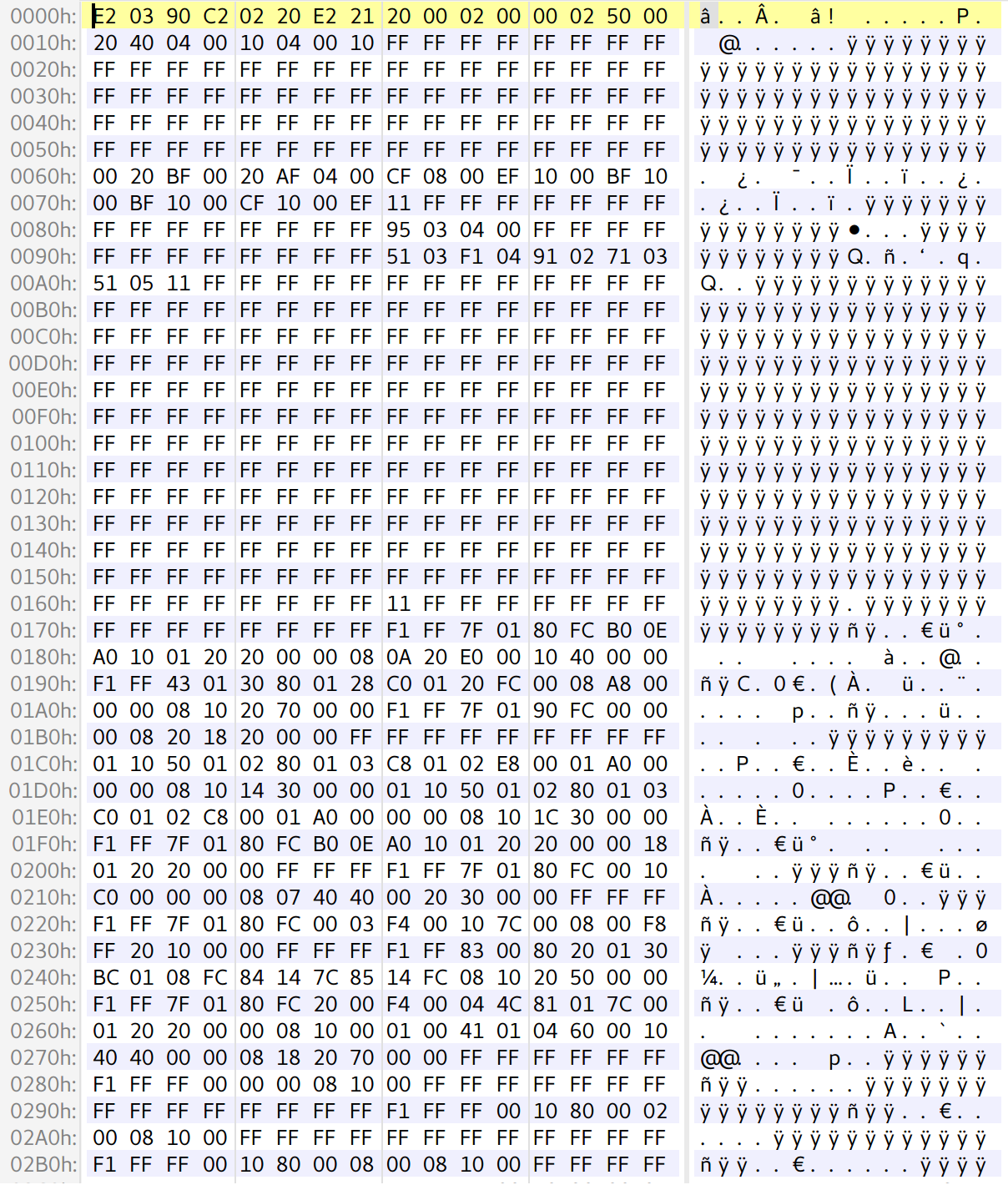
If anybody wants to poke at it, here's the SK-1 ROM dump.

AWS Elasticsearch: a fundamentally-flawed offering