Lessons from Running a Small-Scale Electronics Factory in my Guest Bedroom, part 1: Design
After assembling over 200 Telephreak badges by hand for DEFCON 26 (and taking *way* longer to accomplish it than I estimated) I figured I should document some of the lessons that I learned along the way – from initial design to finished product. The subject of many of the examples of the right way to do things are a small batch of boards I’m currently assembling for Cloud 9 Perception, a friend’s computer vision and robotics company.
This post primarily focuses on design choices for PCBs and the firmware running on them, the next post will show some tricks I’ve learned to save time and energy actually assembling and baking your boards.
There are a number of design choices that really wish I’d considered while making the Telephreak badges. Here are the ones I think would’ve made the most impact to make my life simpler.
Cut some holes in your boards
This one is pretty simple but it can make a big difference. Even if you don’t need to mount your board to anything, adding few holes for alignment purposes can make your life easier in all sorts of ways – primarily when putting together jigs for programming or even mounting through-hole components during assembly. The Telephreak badges *did* have a single hole at the top, but two are really necessary to get decent alignment.
Add proper programming and debugging interfaces
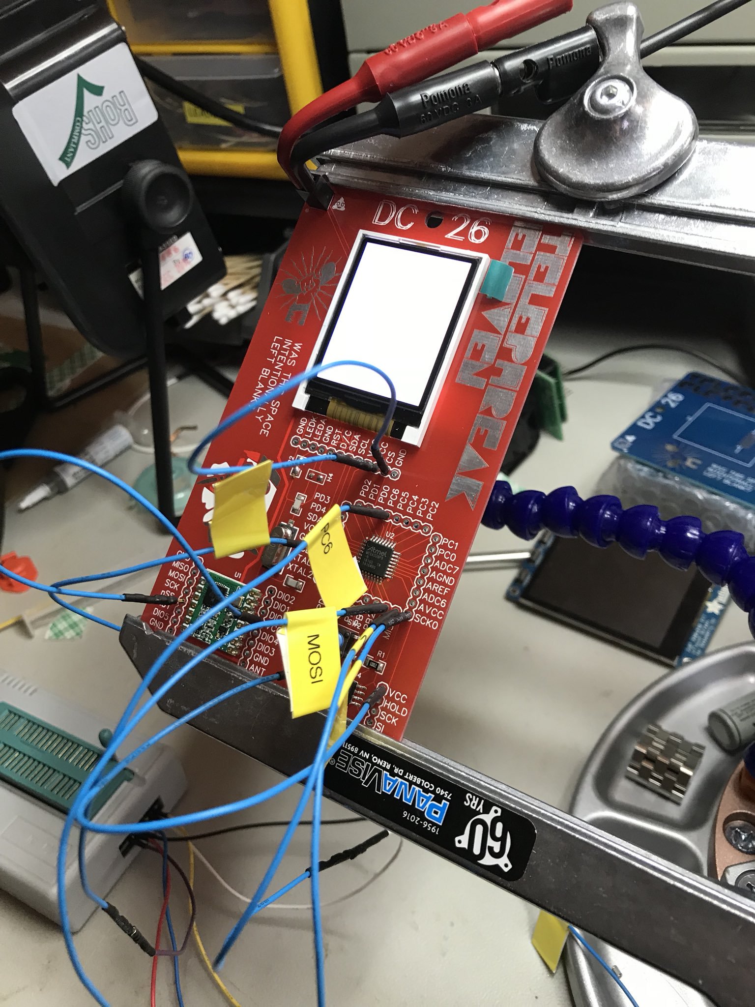
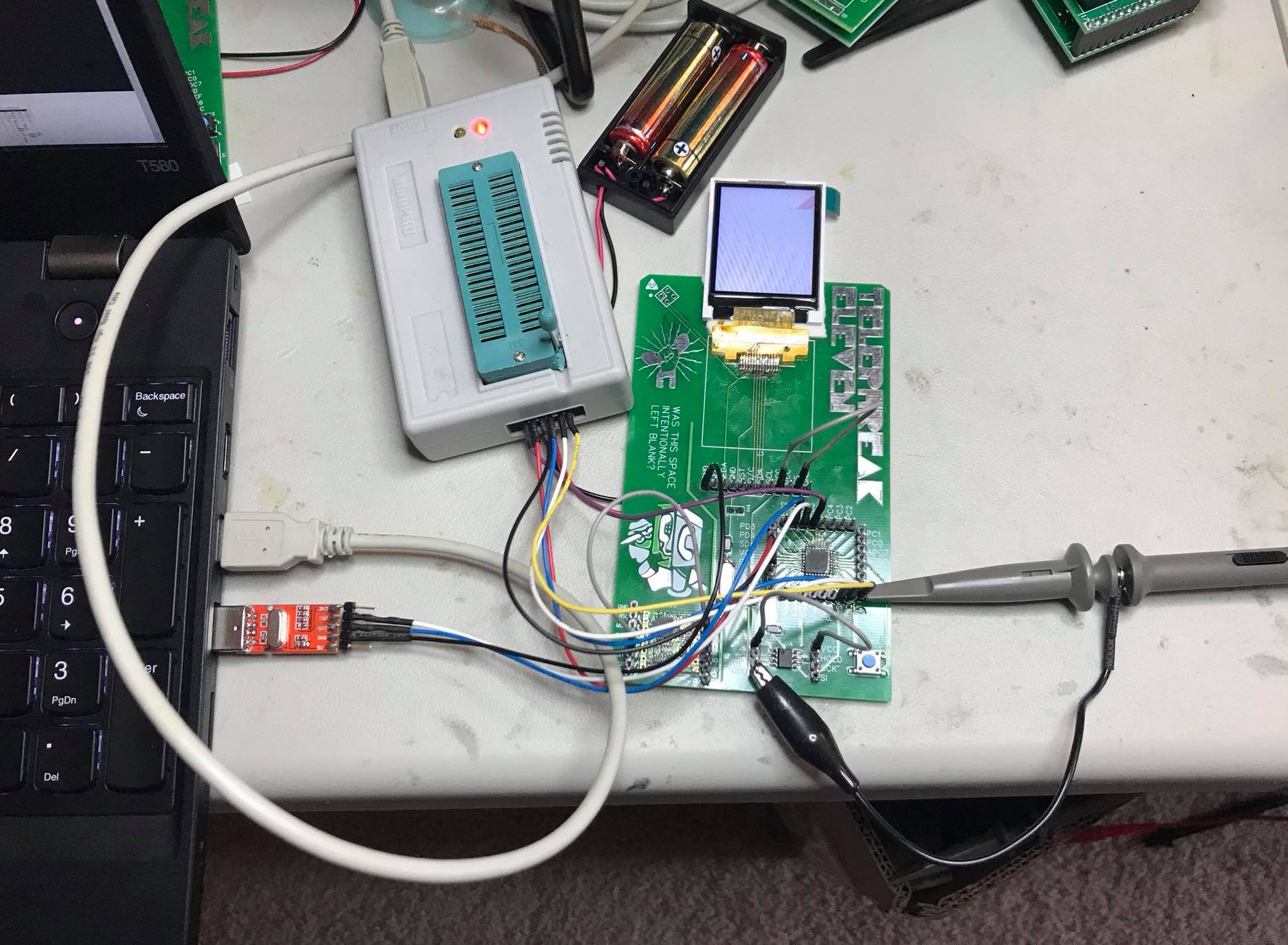
I also really wished I’d added some sort of proper debugging/programming interface to the each of the boards. I had every pin for every device broken out on the board, but I didn’t realize what a pain it would be to reprogram them en masse if the firmware I burned onto the microcontrollers wasn’t perfect. The first step was to forcibly disable 1) the display, 2) the radio, and 3) the flash chip from using the SPI bus by adding three jumper wires to tie their CE pins to VCC. With those three jumper wires in place, the next task was to wire up the four SPI bus lines, the reset line, and VCC and GND. It would’ve been a massive pain to solder wires or pins into the through-holes to do this, even temporarily, so the end result was a bodge of ten leads going to various places on the board, all being held in place by thoughts and prayers.
Next time around, at a minimum, I’ll be adding standard pin headers for the SPI bus, or perhaps even adding a microcontroller and USB port to handle programming.
Align all of your pin headers to be on the same 0.1″ grid
The third thing that would’ve helped would’ve been simply ensuring that the pins I broke out all lined up on the same 0.1″ grid so I could’ve made programming and other jigs by adding pin headers to normal protoboard.
Think about component dimensions
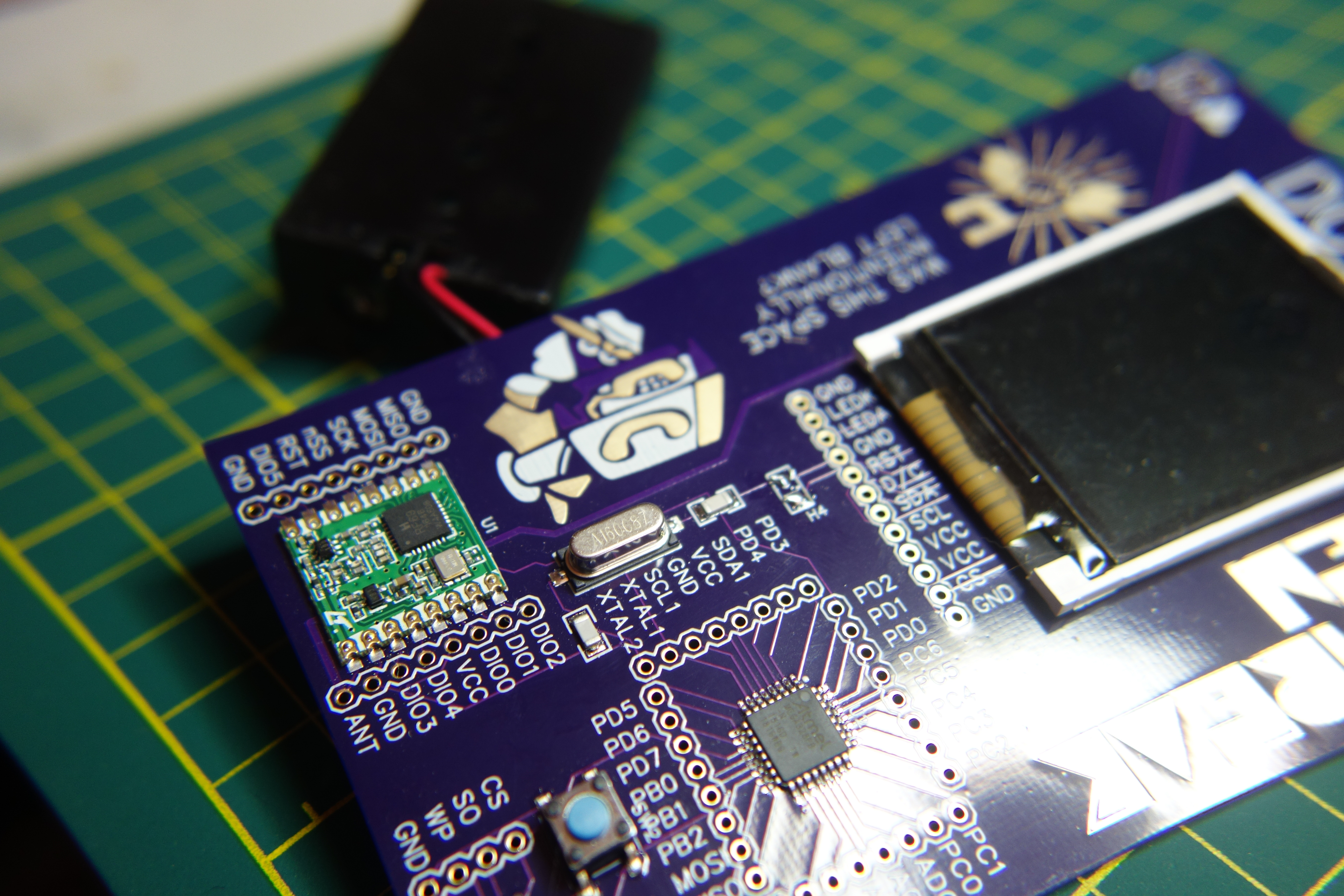
One issue that I saw quite often was that the surface-mount HC49-profile clock crystals were being knocked off, mainly due to being the tallest component on the board. It would’ve been trivial to use a lower-profile component if I’d thought about it beforehand.
Eliminate as many assembly steps as possible
This is a big one. There were two components on the devices that had to be hand-soldered: the battery pack, and the graphic display. For the battery pack, wires had to be trimmed, stripped, tinned, held in place, and then soldered, and the battery pack had to be glued to the board. This ended up being a really tedious process and took up quite a bit of time. Instead, next time for a project like this, I’ll be using battery packs with fixed pins that I can quickly put in place.
As far as the displays, hand-soldering them wasn’t too time-consuming, but it was definitely an error-prone process, and it derived from the fact that I couldn’t bake the LCDs because of temperature issues, and because the flat polyamide cable had to bend backwards and would’ve never held in place. Next time, I’ll add a surface-mount socket for the connector that I can simply bake on with the other components
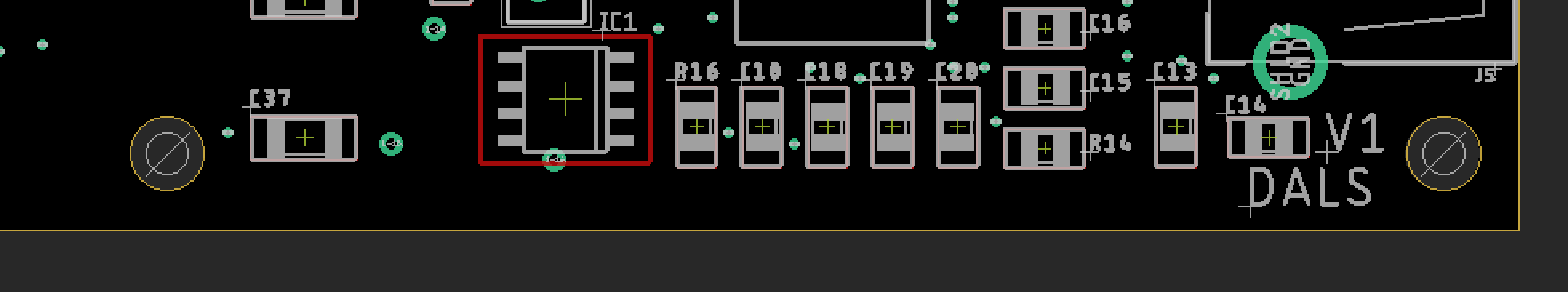
Rename your components once your board layout is finalized

This one is also pretty trivial, but can save a ton of time during assembly if your device has a lot of components. Once your board layout is complete, rename the components so they’re in rough numeric order. This way, when you’re looking for the right spots to place your components, C10 will hopefully be somewhere near C9, and so forth, reducing the amount of space you’re searching for tiny text labels.
Add a test cycle to your firmware
This one would’ve been a big deal for me. The first badges had to wait to receive a radio signal and spend a couple minutes downloading a bitmap over the air before I could confirm that they worked. Not ideal when you’re making 200+ units. Eventually I added a change so I could get *something* on the display at boot to show that it and the microcontroller were alive, but the radio and flash chip weren’t tested.
The Cloud 9 boards I’m working with have a full test cycle, and by using LEDs along with relays, you can actually get audible feedback that things are working. It tests all of the hardware, including Ethernet and the camera, and will deliver some very satisfying relay clicks as tests complete successfully (or give you an idea of where the problem is if something isn’t working correctly)
Coming next, my favorite part… assembly!
Getting into the Pace 5268AC Router, part 3: Sacrifices Must be Made (to the JTAG gods)

Everything Always Returns 0: Adventures in Adding “Volkswagen Mode” to FreeBSD