Lessons from Running a Small-Scale Electronics Factory in my Guest Bedroom, part 2: Assembly
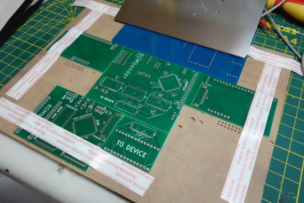
Our parts have arrived and our boards are ready; let’s build some electronics!
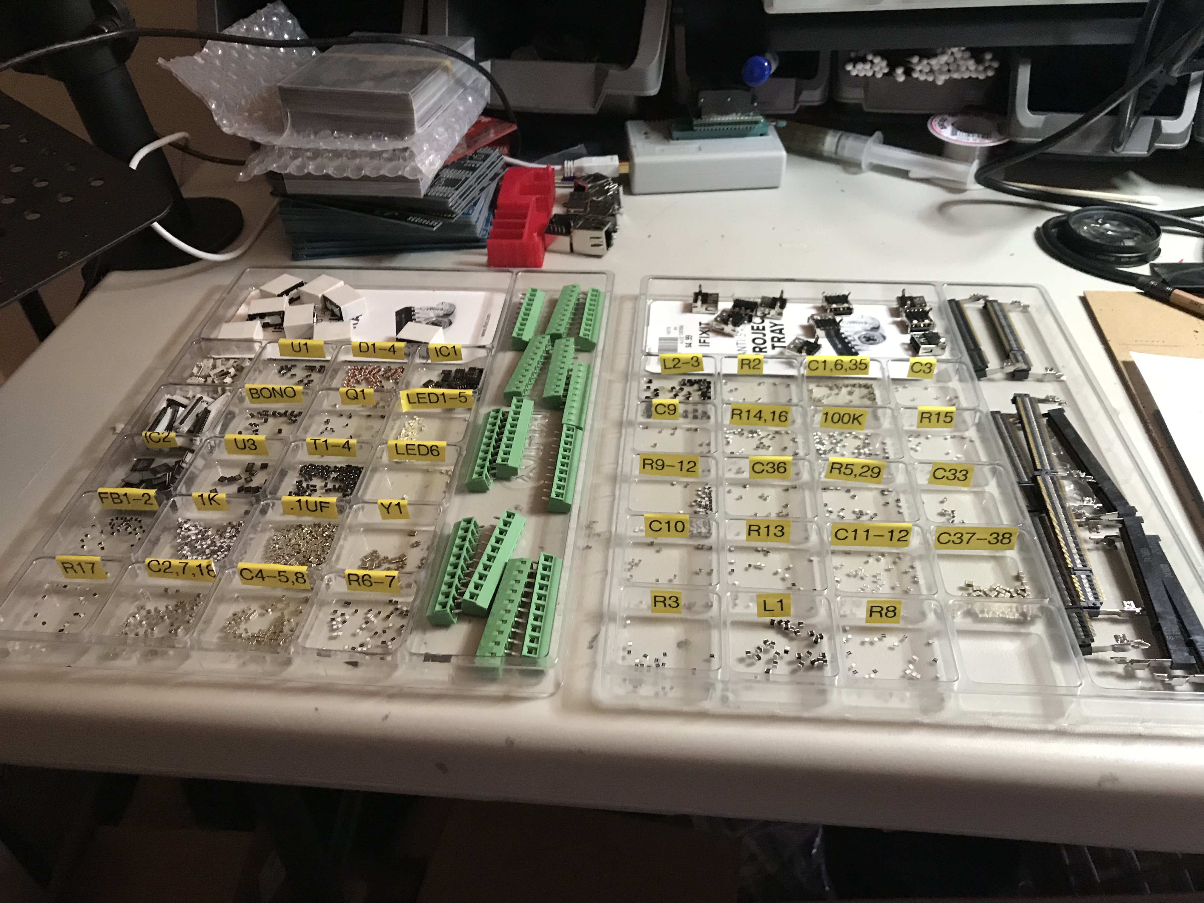
The first step is to get things organized. I love the iFixIt Project Trays for keeping components organized. My general methodology is to label components in the trays based on their identifier on the board. One thing I really try to keep in mind when organizing parts is to keep similar-looking components away from each other, especially unlabeled ones like capacitors and inductors. The reason for this is that when I drop a part (which happens often) I don’t want it to fall into a space with a different part that looks identical, thus forcing me to measure every component in that space in the tray.
Another useful detail about these trays is that they seal fairly well when stacked. When I leave my bench, I’ll stack them all together (with an empty one on the top) and tape them together to prevent catastrophe if my cat decides to hop up on my bench and knocks things over.
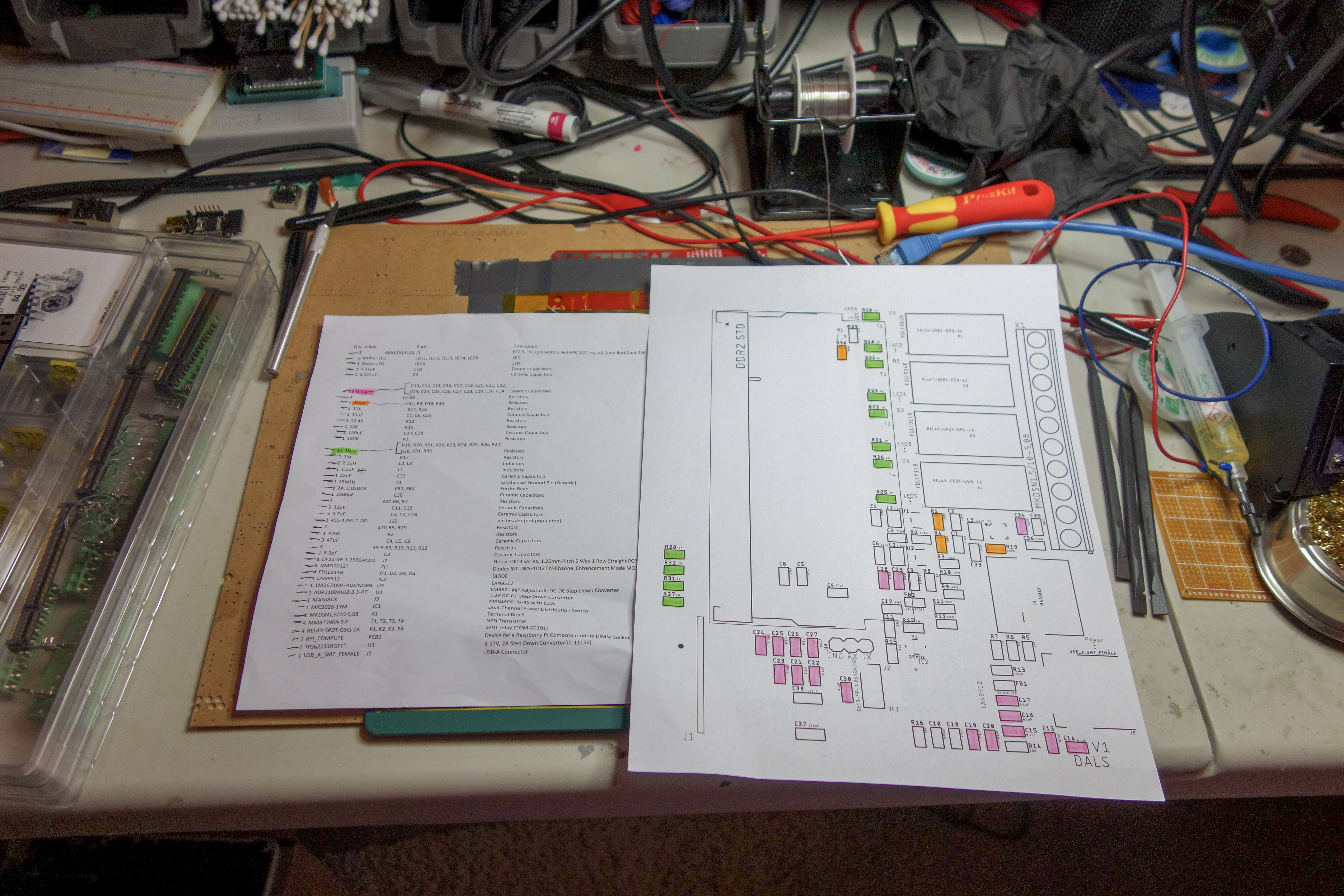
When a component is used in too many places to fit on a label, I label it by value instead and use a printout of the board layout and bill of materials to make it easy to place them. This really saves a ton of time when searching for spots to place components.
Once we’ve got our parts organized, the next step is to prepare a jig for stenciling with solder paste. I generally just tape down spare/bad PCBs around all four sides of the first board I’m assembling, making sure that all sides are flush and everything is secure. After that, I am VERY careful to align the stencil with the PCB, and then I tape one side of it down as well.
Board is held in all four directions 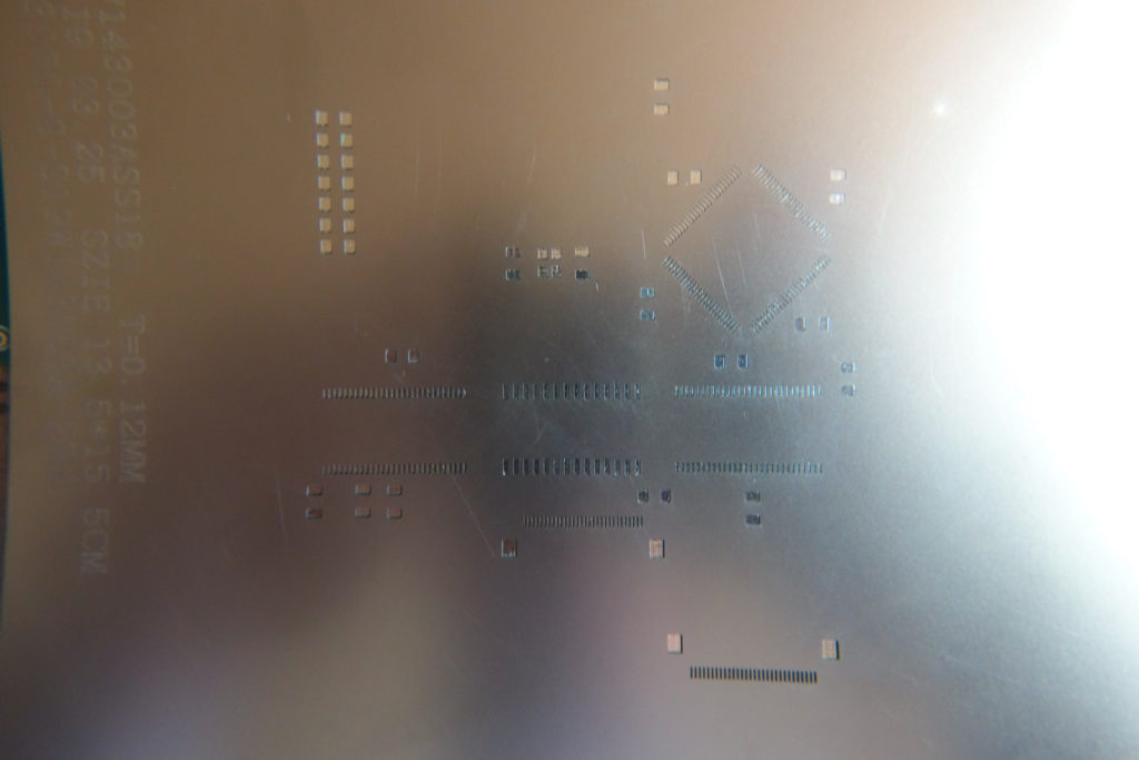
Stencil is accurately lined up with PCB 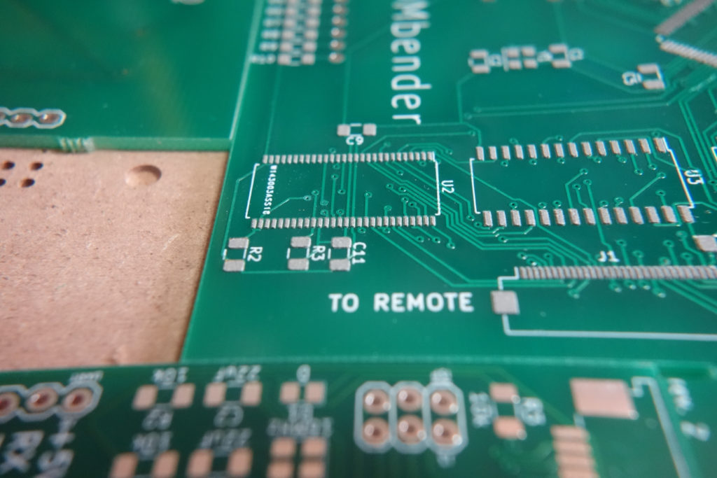
We end up with a clean and accurate layer of solder paste on each pad
Now we’re ready to do some actual stenciling. SparkFun’s tutorial video is pretty good but there are a couple things that I think are worth pointing out.
Solder paste in tubs is a bit of a pain and I generally opt for syringes. Solder paste that comes in syringes is much more consistent and lasts longer because of less exposure to air and it’s generally easier to deal with.
If you do use a tub, it’s common to have to stir up your solder paste to mix up the top layer that’s dried. Sometimes you may even need to add additional flux as the paste ages, but be careful not to add too much or it can become runny and you won’t be able to stencil with it.
I also generally try to apply paste to my boards with only one swipe. It works well if you have enough paste on your putty knife and it’s wider than the board you’re working with. The main reason is that each swipe you make across the stencil can slightly move things and make the paste smudge a bit.
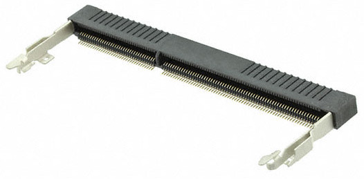
One final note about stenciling – if you have a component with a lot of fine pins in one direction that can tend to bridge (like a SODIMM socket for example) if you’re able, it works best to swipe parallel with the pins of the device instead of perpendicular.
From here, we populate the board with our surface-mount components. I’ve used vacuum tools before, but I generally prefer a simple pair of angled tweezers. I also like a small hobby/X-ACTO knife to help adjust alignment of components once they’re already on the board.
Try to let your components “rest” on top of the solder rather than pressing them down into it. One of the really cool things about this process is that the surface tension of the molten solder and flux will help pull your components into alignment if it’s not perfect. You should still try to be as accurate as possible, and having a very clean stencil job will help a lot here. With components resting on top of the solder, their pins get “sucked” down into it as the solder liquefies.

Components are placed 
Great alignment after baking
(one pin got some touch-up after this photo)
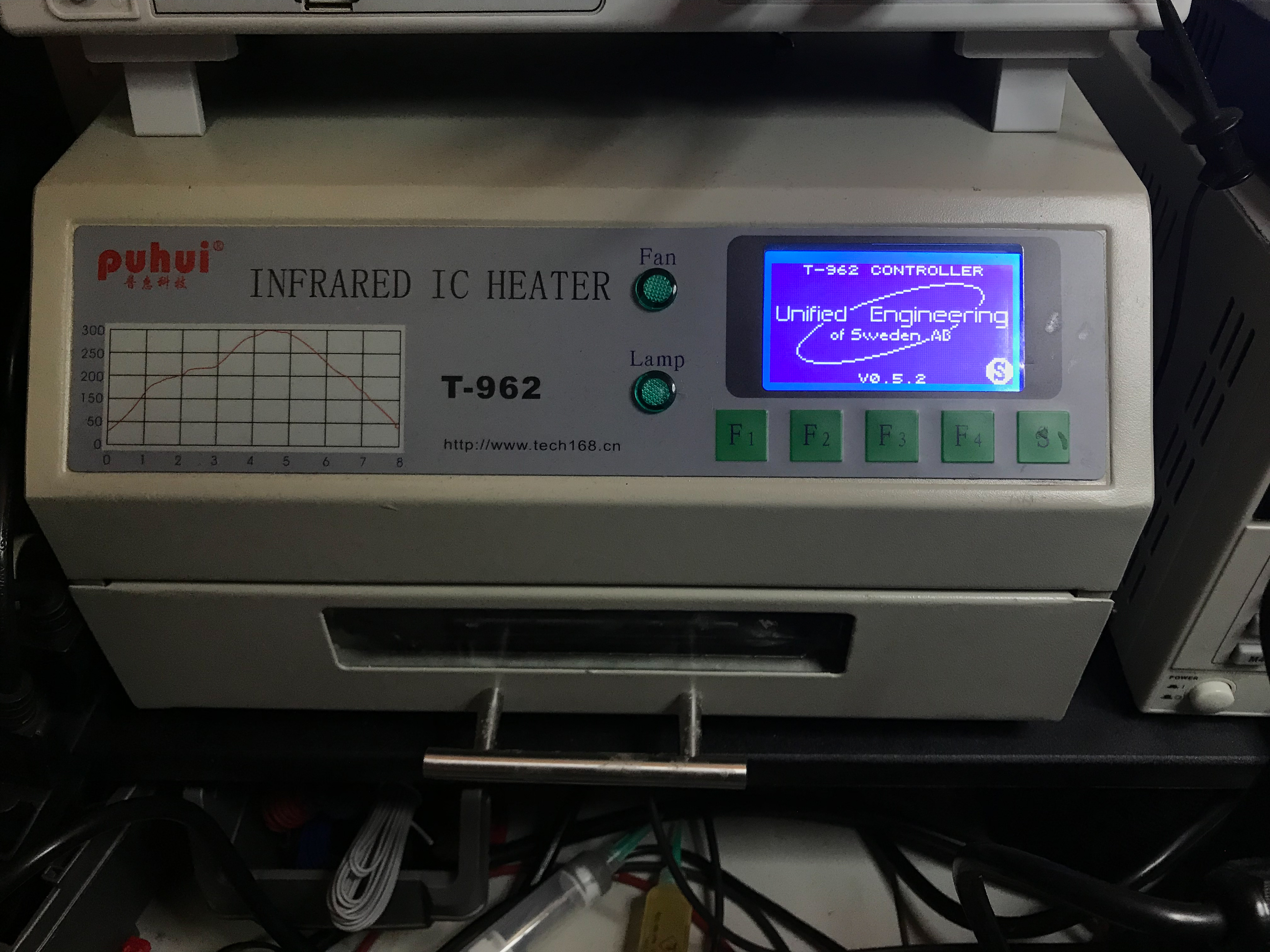
Once the surface-mount components have been placed, it’s time to bake the board. I’ve had really good luck with the cheap T-962 reflow oven after performing the simple mods listed at https://github.com/UnifiedEngineering/T-962-improvements. I haven’t really had to deviate from the reflow profiles specified in the datasheet for whatever solder paste I’m using at the time.
I always dislike dealing with through-hole components after baking a board. Unless you glue the component to the board or bend its pins, they’re often awkward to hold in place and keep level while they’re upside-down on one side of the board. Simultaneously, you actually have to solder them on the top side. In plenty of situations, you can’t simply set the board down on top of the components either due to their location or shape.
What I’ve started doing is 3D-printing jigs for the through-hole components that are a pain to deal with. Autodesk EAGLE will let you export boards into Fusion 360, and KiCAD can do the same with FreeCAD. From there, it’s pretty simple to use the component footprints as a template to design and print a jig.

Fusion 360 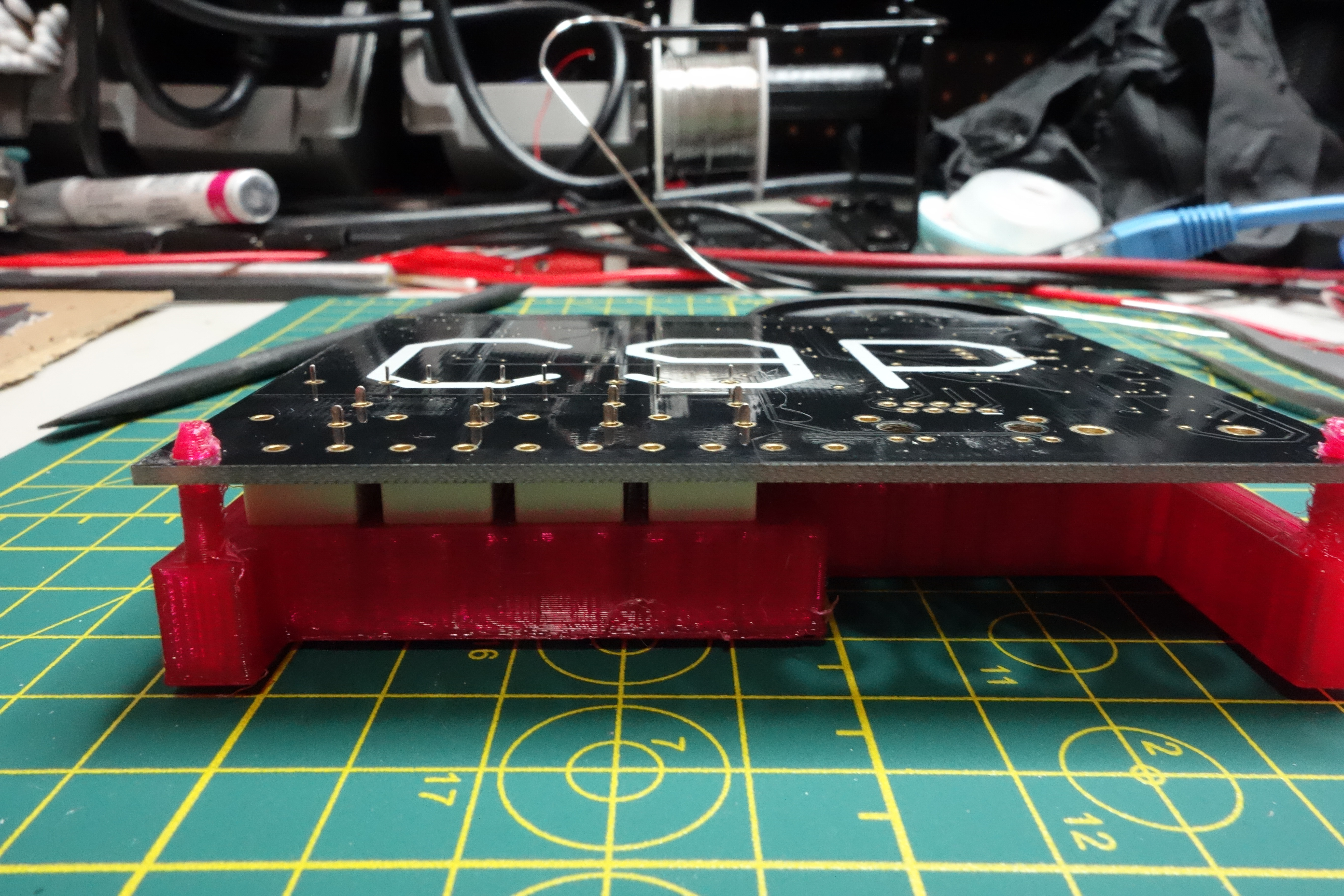
Real-life!
One thing I’ve found that also helps for this part of the process is to only work with one type of component at once, and to leave a generous amount of space between the body of the jig and the PCB. This helps ensure that components end up flush against the board.
At this point if everything went to plan, we’re done. If not, the first thing I do is check for solder bridges. I use an inexpensive USB microscope to get a better view of what I’m doing if I do find anything was bridged. Usually I can just add a bit of flux and use a soldering iron to take care of any bridges. The Chipquik flux is great and you can find it at a lot of shops, but if you need something heavy-duty, the Amtech stuff is hard to beat. Baking the board a second time is always worth a shot as well – unless you’ve added through-hole components that will melt in the oven – that’s particularly an issue with electrolytic capacitors, relays, and pin connectors. If something’s really problematic, occasionally I’ll add some extra flux to the board and bake it again, but that’s rare
I hope you found this interesting or useful and I’d love to hear any feedback and thoughts!

AWS Elasticsearch: a fundamentally-flawed offering
OpenCL in FreeBSD jails (AMD GPU passthrough)